PAP Technology Developed by JTEC Corporation
PAP(Plasma Assisted Polishing )
This technology utilizes plasma to activate and polish surfaces, specifically designed for polishing hard materials such as diamond. Compared to conventional mechanical polishing using diamond abrasives, it offers higher efficiency while preventing the formation of processing-induced damage layers. This technology is gaining significant attention for its potential in the polishing process of diamond substrates, which are expected to play a crucial role in next-generation power devices.
Strengths of PAP Technology
POINT
High-efficiency, high-precision polishing
Achieves both high processing speed and precision at an advanced level
POINT
No processing-induced alteration layer
Preserves crystal structure integrity and prevents surface damage, enhancing product reliability and performance
POINT
Environmentally conscious
A fully dry process that does not use chemicals or polishing slurry, contributing to reduced environmental impact.
Advantages
The PAP (Plasma Assisted Polishing) Equipment is designed to achieve high-efficiency and damage-free polishing by utilizing plasma-activated particles (ions and radicals) that chemically bond with the atoms on the surface of the workpiece, weakening the interatomic bonds. This enables high-precision processing of ultra-hard materials such as diamond, which has been challenging with conventional mechanical polishing methods.
Wide Applicability
Applicable to hard materials and new materials beyond diamond, providing equipment for a wide range of phases from research and development to mass production.
Shortened Polishing Time
Reduced Polishing Time for Improved Efficiency
Cost Reduction
By adopting a simple design, equipment costs are reduced, and slurry-free operation lowers running costs.

Application Examples
Devices made from hard materials such as diamond and silicon carbide (SiC) exhibit excellent thermal efficiency due to their high thermal conductivity and low thermal expansion coefficient, allowing them to operate at high temperatures without losing efficiency. As a result, heat dissipation design becomes simpler, and durability and reliability at high temperatures are enhanced. This technology is expected to be increasingly utilized in various fields, including semiconductors, electronics, aerospace, medical devices, renewable energy, laser technology, and transportation sectors such as automobiles and trains.
Application to Hard-to-Process Wafers
(e.g., Diamond)
Application to Power Devices: Contributing to the performance enhancement of next-generation power devices by applying to high-quality SiC wafers and diamond substrates.
Application to Optical Components: Suitable for manufacturing high-precision diamond lenses and windows.
Application to Diamond Heat Dissipation Substrates
Application to Heat Sinks: Diamond substrate heat sinks are attracting attention as highly effective cooling solutions due to their excellent thermal conductivity and high durability.
Application to Mechanical Uses of Diamond
Application to Mechanical Uses: Diamond, with its excellent wear resistance and anti-adhesion properties, is gaining attention for use in tools, molds, and sliding components. Additionally, improved machining precision and defect reduction are expected to lower costs and extend product lifespan
Technology Application Examples
Power Devices
Diamond substrates contribute to improving the efficiency and reliability of power devices due to their high thermal conductivity and pressure resistance. Additionally, the exceptional properties of diamond enable stable performance even in harsh operating environments.
Despite their advantages, diamond substrates face challenges for practical application, including cost, machining difficulty, bonding technology, and thermal expansion issues. However, in terms of machining difficulty, PAP (Plasma Assisted Polishing) has achieved clean, high-efficiency polishing without generating a processing-induced altered layer.
Application
・Power Electronics: Power MOSFET (Metal-Oxide-Semiconductor Field-Effect Transistor), IGBT (Insulated Gate Bipolar Transistor)
・Power Conversion Devices: Power conversion devices for solar power generation systems and wind power generation systems.
・Electric Vehicles (EV) and Hybrid Electric Vehicles (HEV): Inverters and power control units for electric and hybrid vehicles
・High-Frequency and High-Power Communication Equipment: High-frequency communication devices and high-power communication systems (such as radar systems and satellite communication devices)
・High-Power Laser Systems: High-power laser equipment and laser-guided systems
Heat Sink
Heat sinks made of aluminum or copper substrates have been commonly used. However, in electronic devices with high thermal loads, as well as in specialized applications, cooling systems tend to become complex and large-scale. On the other hand, using diamond heat sinks provides a simple and efficient solution.
Despite its superior properties, the use of diamond has been limited due to its high cost and machining difficulties. However, PAP (Plasma Assisted Polishing) has enabled clean, high-efficiency polishing without inducing processing-induced damage layers. This technology expands the potential for the practical application of diamond substrate heat sinks.
Application
・High-Performance Electronic Devices: High-performance semiconductor devices and integrated circuits (ICs)
・Laser Equipment: High-power laser systems and laser diodes
・High-Power Electrical Equipment: Power electronics (such as high-power transistors and power MOSFETs)
・Aerospace and Satellite Technology
・Medical Equipment: Medical devices requiring precise cooling (such as MRI and CT scanners)
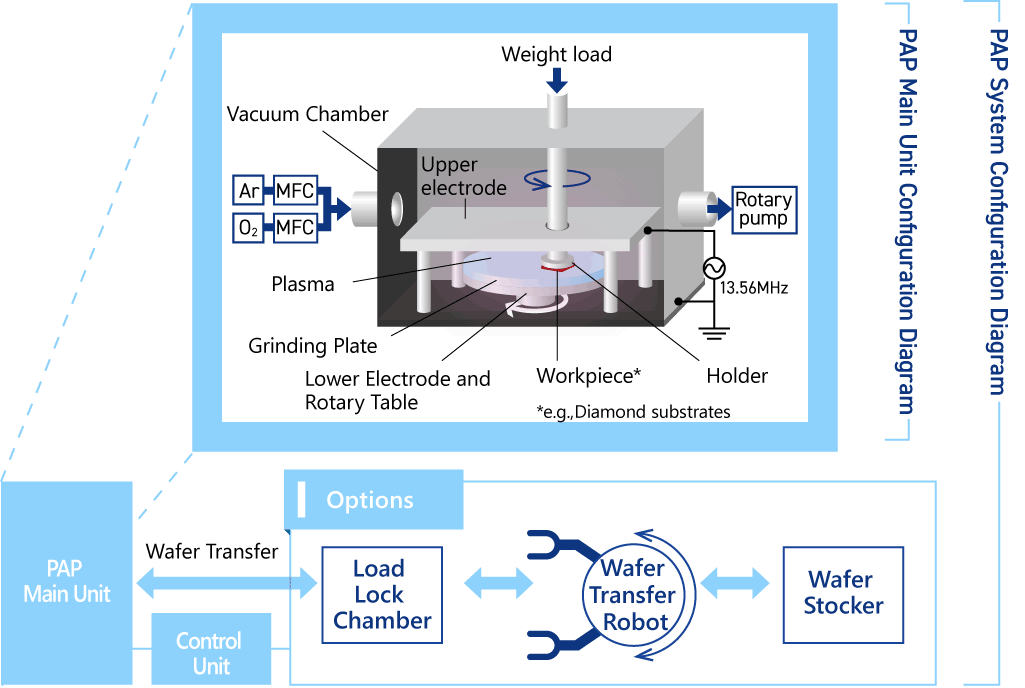
Processing Overview
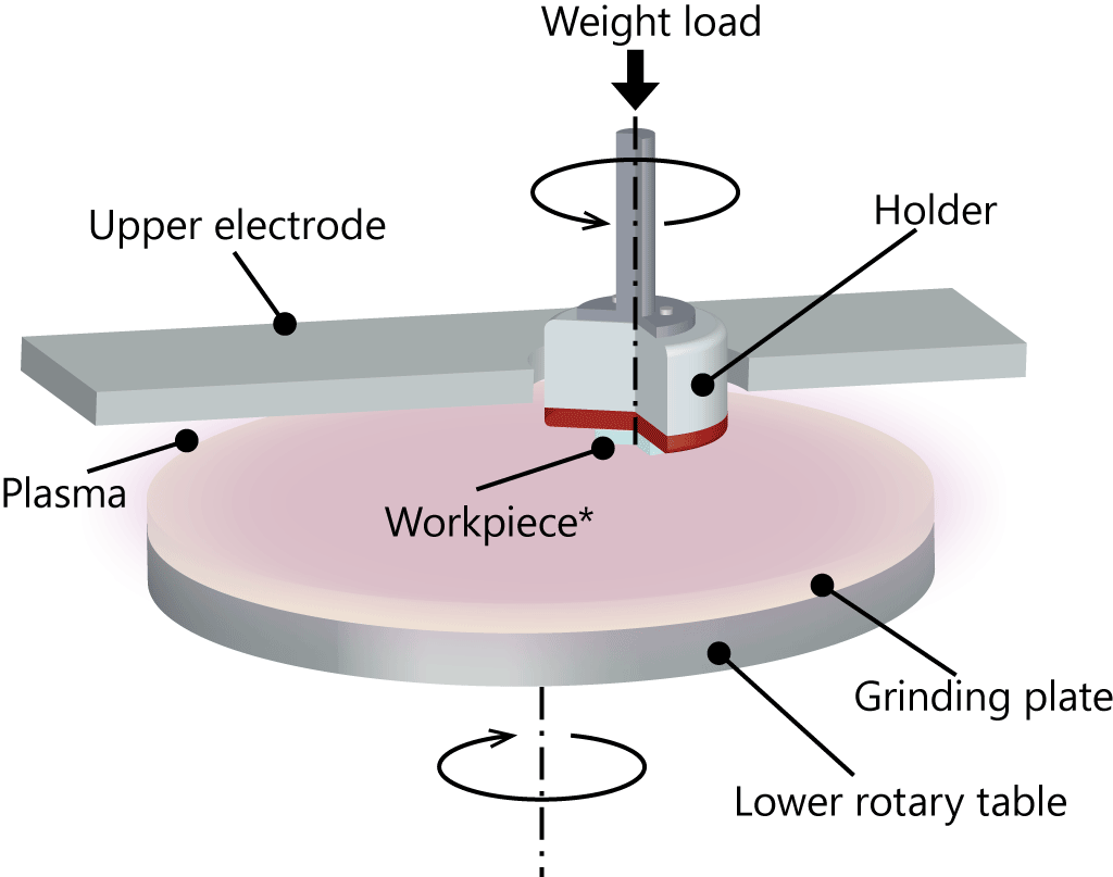
*e.g.,Diamond substrates
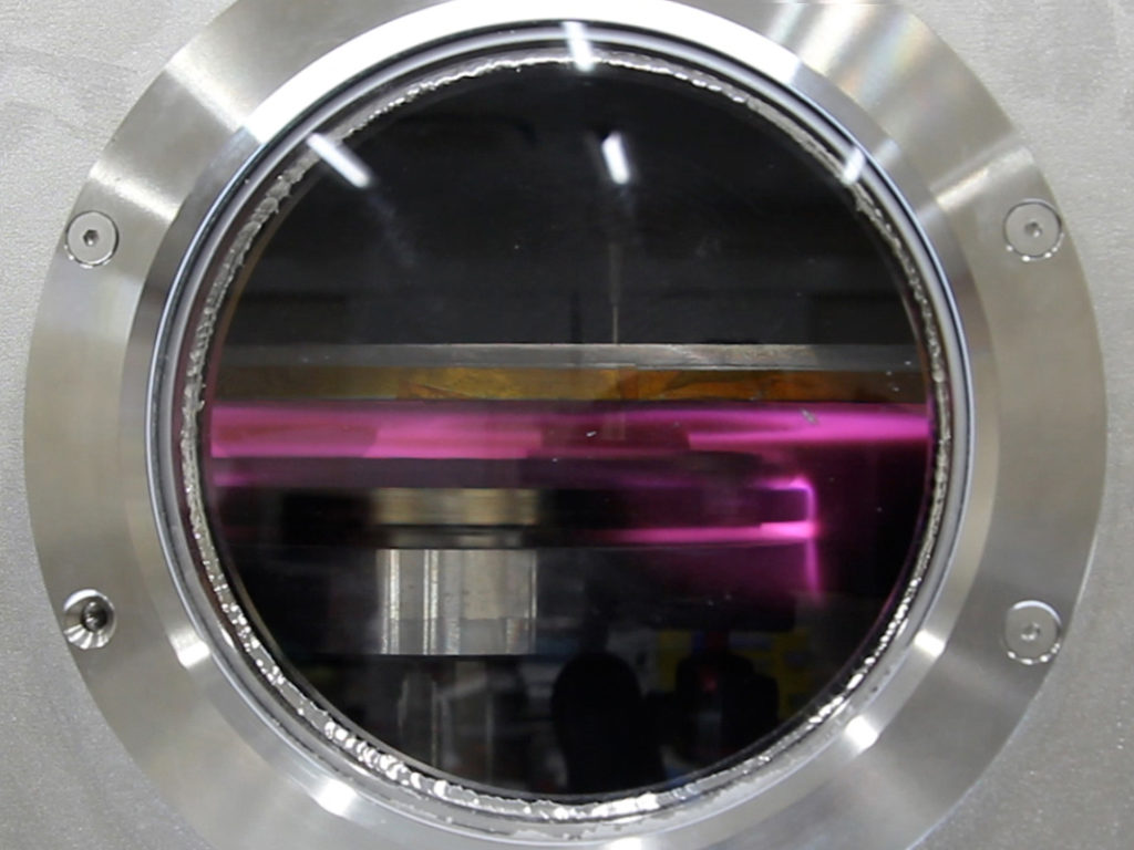
Plasma-Induced Surface Modification
The reason why even hard materials can be processed is that the plasma on the processing table chemically bonds strongly with the atoms on the surface of the workpiece (such as a diamond substrate), thereby breaking the bonds between the surface and the internal structure of the workpiece.
Polishing Process
Since this is a dry process that does not use diamond slurry or polishing plates typically used for hard materials, it creates a smooth surface without defects or processing-induced damage.
The surface roughness of single-crystal diamond substrates is significantly improved
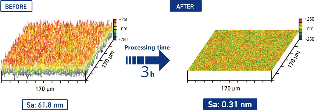
By applying PAP (Plasma Assisted Polishing), the surface roughness (Sa value) of diamond substrates is greatly improved from 61.8 nm to 0.31 nm.
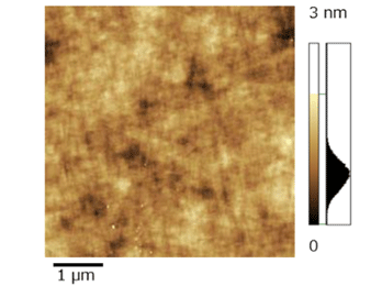
Measurement by Atomic Force Microscopy (AFM)
The root mean square roughness after polishing was measured at 0.36 nm, confirming an extremely smooth surface.
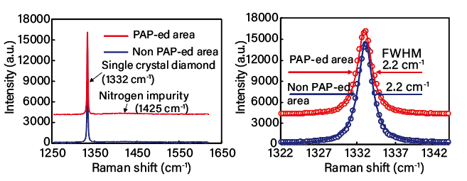
Measurement by Confocal Raman Microscopy
Confirmed no disruption in crystallinity or transition to a graphite structure, achieving damage-free polishing.
Comparison with Conventional Polishing Methods and Their Advantages
| Issues |
Advantages of PAP (Plasma Assisted Polishing) |
|
|---|---|---|
| Comparison with Mechanical Polishing Methods The mechanical polishing method is a polishing method that physically removes material using hard abrasives such as diamond grit. |
[Low Polishing Efficiency] [Surface Damage Occurrence] |
[High-Efficiency Polishing] [Damage-Free Polishing] |
| Comparison with Chemical Mechanical Polishing (CMP) Method CMP is a method that combines chemical etching and mechanical polishing, mainly used for planarizing semiconductor wafers. |
[Environmental Impact] [Difficulty in Application to Hard Materials] |
[Environmentally Friendly] [Specialized for Hard Materials] |
| Comparison with Ion Beam Polishing Method The ion beam polishing method is a polishing method that removes material by irradiating the material surface with an ion beam. |
[High Equipment Cost] [Slow Polishing Speed] |
[Cost-Effective Equipment] [High Polishing Speed] |
| Comparison with Laser Processing Method The laser processing method is a processing method that uses a high-power laser to evaporate or sublimate materials. |
[Thermal Effects] [Surface Quality Limitations] |
[Low Thermal Impact] [High-Quality Surface] |
Product Features
PAP (Plasma Assisted Polishing) offers a significant advantage over competing polishing methods by enabling highly efficient, damage-free polishing of hard materials. This provides the following benefits:
・Improved Product Quality: High-quality surface finishing enhances the product’s performance and reliability.
・Improved Productivity: Faster polishing speeds improve production efficiency.
・Cost Reduction: Shorter polishing time and reduced environmental impact lead to overall cost savings.
・Environmental Compliance: No chemicals are used, ensuring compliance with environmental regulations and enhancing the company’s image.
Steps to Equipment Installation
STEP

Inquiry
Accepting inquiries about PAP (Plasma Assisted Polishing) technology and equipment.
STEP

Technology Introduction
Visit or Web meeting based on your preference.
STEP

Sample Polishing and Evaluation
Test polishing and evaluation cycles are conducted as needed.
STEP

Proposal for Estimated Cost and Equipment Specifications
Proposal based on needs and test polishing results.

Proposing the optimal system tailored to your needs.
If you have any inquiries or need more detailed information, please feel free to contact JTEC Corporation.
Example of Main Unit Configuration
Equipment Specifications
| PAP(Plasma Assisted Polishing Method) | PA1100 | |
|---|---|---|
| Basic Specifications | Worktable Material | Quartz, etc. (Diameter: 240 mm) |
| Workpiece Size | Flat: Maximum diameter 4 inches, Thickness: 0.4 mm – 20 mm | |
| Plasma Power Supply | Maximum 1 kW | |
| Process Gas | Ar、 O2 | |
| Vacuum Level (During Processing) | Ultimate vacuum: 20 Pa | |
| Control Unit | Programmable Logic Controller (PLC) | |
| External Dimensions | W1400 mm × D800 mm × H1900 mm | |
| Mass | Approx. 400 kg | |
| Utilities | Power Supply | Three-phase AC 200V, 20A / Single-phase AC 100V, 15A |
| Instrument Air | 0.4~0.6MPa | |
※For workpiece size, please consult us.
Company Profile
| Company Name [Trade Name] | JTEC Corporation |
|---|---|
| President and Representative Director | Takashi Tsumura |
| Description of Business | Design, manufacture and sales of X-ray mirrors for synchrotron radiation facilities Development, design, manufacture and sales of automated cell culture system Development, design, manufacture, and sales of various automated systems Development, manufacturing, and sales of surface processing of various materials Support services related to regenerative medicine |
| Capital stock | 847,148,000 yen (as of June 30, 2025: consolidated) |
| Established | 1993/12/21 |
| Location of head office | 2-5-38, Saito Yamabuki, Ibaraki, Osaka 567-0086, Japan |