JTEC Corporation’s Plasma CVM Technology
Plasma Chemical Vaporization Machining
(Plasma CVM)
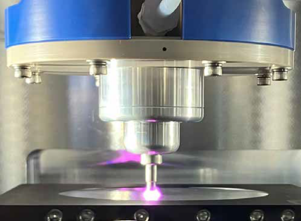
JTEC Corporation provides innovative solutions in semiconductor and quartz wafer planarization processing using Plasma Chemical Vaporization Machining (Plasma CVM) technology. Plasma CVM is a technology with excellent features of nano-level processing accuracy and no process alteration layer (no damage to the surface of the workpiece).
Advantages of our Plasma CVM
POINT

Numerical Control Technology
Nano-level processing accuracy
High-precision planarization process
Reduction of thickness variation
POINT

Atomic-scale processing
No process alteration layer is generated(Damage-less)
Contribution to quality improvement and electrical characteristics
POINT

Chemical reaction
Suitable for various wafers
Crystal (SiO2), silicon (Si),
SOI, GaN, etc.
Advantages of Plasma CVM
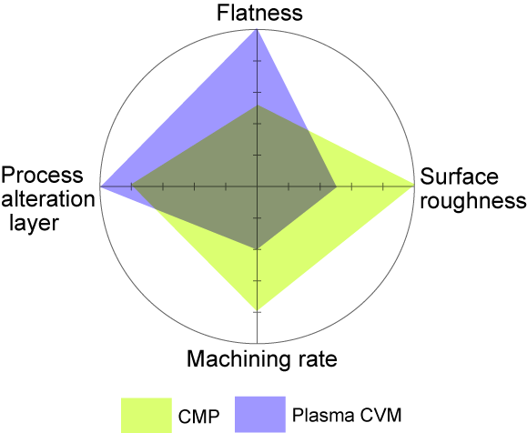
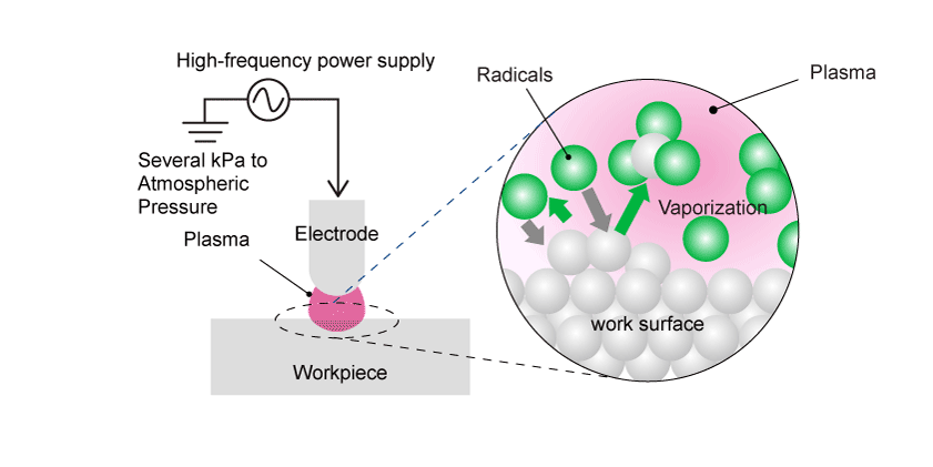
Plasma CVM is a unique technology that uses only chemical reactions as its processing principle, which is distinct from CMP and ion beam processing, which remove by mechanical action. Plasma CVM achieves high-precision planarization that cannot be achieved by CMP and does not cause damage as ion beam processing does. Plasma CVM can contribute to process simplification and cost reduction, as post-processing cleaning may not be necessary depending on the subsequent process.

Improvement of wafer performance
Further planarization of wafers after CMP

Improved wafer quality
Provides a high quality surface without the worry of process alteration layer

Reduces wafer manufacturing costs
Contributes to cost reduction by simplifying the process

Complementary relationship with CMP
Plasma CVM significantly improves the planarity of wafers polished by CMP.
By combining CVM and CMP in a complementary process, wafers of higher quality than ever before can be obtained.
Polishing by CMP
Polishes wafer surfaces to improve roughness, high polishing rate
Plasma CVM for better planarity
Improvement of wafer flatness by numerically controlled processing, removal of process alteration layer generated by CMP
Environmental Considerations
Plasma CVM is a wafer processing by gas phase chemical reaction, and although exhaust gas treatment is necessary, it does not use chemicals that incur wastewater treatment costs.
It is a solution that realizes high-quality, high-performance wafers in a dry environment.
Please click the button below to contact us with any questions or for more information.
Principle of Plasma CVM that realizes atomic-scale processing
Excellent processing efficiency
Chemical reactions using high-density neutral radicals from high-pressure plasma enable processing with higher processing efficiency than conventional plasma etching, contributing to higher productivity.
Atomic-scale high-precision processing
Plasma CVM can generate plasma locally, enabling machining with high spatial resolution. This makes it an excellent match for numerically controlled machining, and it achieves excellent planarization of wafers through atomic-scale high-precision machining.。
Realizes damage-free wafer processing surface
Plasma CVM, which is characterized by processing by chemical reactions, does not produce a process alteration layer on the processed surface of the wafer. This contributes to higher quality and performance of electronic components using wafers processed by Plasma CVM.
Examples of Plasma CVM Processing
Quartz crystal
Pre-processed quartz wafer: 4-inch (100 mm)/commercially available
Measurement range: Area within a circle of 100 mm diameter
BEFORE
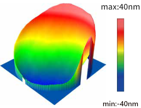
Pre-processing thickness distribution
TTV: 102 nm
AFTER
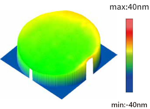
Thickness distribution after processing
TTV: 18 nm
SOI
Pre-processed SOI wafer: 8-inch (200 mm)/commercially available
Thin film SOI wafer (SOI layer: 100 nm, embedded oxide layer: 200 nm)
Measurement points: Area within a 190 mm diameter circle, 5.5 mm grid
BEFORE
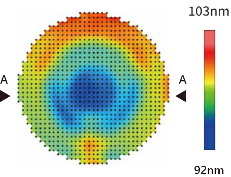
Thickness of SOI layer before processing
Average thickness: 97.5 nm
TTV: 9.4 nm
AFTER
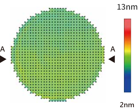
Thickness of SOI layer after processing
Average thickness: 7.5 nm
TTV: 3 nm
Improvement of TTV of quartz and SOI by nano-level control
TTV: Total Thickness Variation
The difference between the maximum and minimum thicknesses in the flatness application area of a wafer
Introduction of Plasma CVM Systems
Proposal for further improvement of quality and performance of various types of wafers
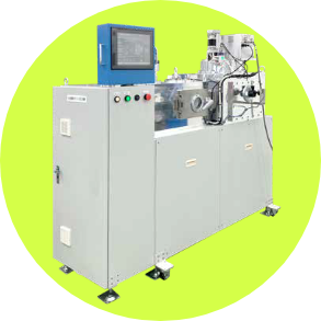
(Standard type for development and small-lot production)
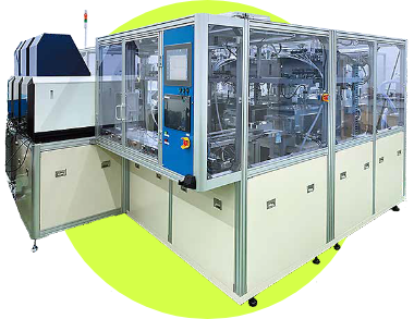
(Fully automated type for mass production)
Improved productivity
All processes, from wafer removal from the cassette, thickness measurement, processing, and data storage, are automated. Efficient production is possible without manpower.
Cost Reduction
Compact design minimizes He gas usage and significantly reduces running costs. This system is also environmentally friendly.
Reliable Traceability
All thickness data before and after processing is stored in the system. Quality control is assured.
Features of Plasma CVM Products
■JC100
Stand-alone type
(Standard type for development and small-lot production)
・Stand-alone type
・Suitable for customers who wish to independently study Plasma CVM
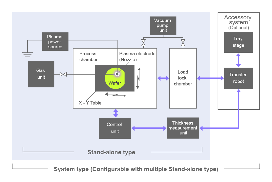
・Load-lock chamber reduces the time required to change samples and enables efficient continuous processing.
・Thickness measuring device is included.
■JC2000
System type
(Fully automatic type for mass production)
・Equipped with a processing unit and a measuring unit, this automatic system calculates the amount of processing based on the measurement data and performs processing.
・System configuration for mass-production processing
・Wafer transfer in the system is performed by transfer robot.
・High throughput is achieved by using multiple processing chambers (two chambers for JC2000).
Steps up to System Installation
STEP

Inquiry
Accepts questions regarding Plasma CVM technology, system, etc.
STEP

Technology introduction
Visit or web conference, depending on your request
STEP

Sample prototyping and evaluation
Test processing is available at any time
STEP

Proposal for rough estimate, detailed system specifications, etc.

We propose the optimal system to meet your needs.
Plasma CVM system consists of a process chamber for processing, a load lock chaber, and a thickness measurement unit.
We can propose optimal system configurations for customers seeking to improve processing capacity and shorten takt time.
If you are interested in producing high-quality, high-performance wafers efficiently and at low cost, please click the Inquiry button below to tell us about your needs.
Plasma CVM System Configuration Example
Plasma CVM system general specifications
| Plasma Chemical Vaporization Machining (Plasma CVM) |
JC100 (Plasma CVM processing system) | JC2000 (Plasma CVM automated machining system) | |
|---|---|---|---|
| Basic configuration | Process chamber | 1 chamber configuration with plasma electrode | 2 chamber configuration with plasma electrode |
| Load lock chamber | 1 chamber configuration | 2-chamber configuration | |
| Degree of vacuum | Achievable vacuum 10 Pa | ||
| Gas type | He / SF6 for process, N2 for purge | ||
| Plasma power source | 13.56 MHz / Max. 300 W | ||
| Control unit | PLC control (partly PC control) | ||
| Thickness measurement unit | Spectral interferometry (for wafer thicknesses from 20 to 100 µm) | ||
| Peripheral system (Option) |
Tray stage | - | Multi-stage loading of trays up to 4-inch size |
| Transport Robot | - | 4-axis (X-axis, Y-axis, Z-axis, θ-axis) robot | |
| Dimensions | W2000 mm × D750 mm × H1600 mm | W2000 mm × D3700 mm × H2200 mm (2-chamber configuration) | |
| Weight | Approx. 1000 kg | Approx. 2500 kg (2-chamber configuration) | |
| Utility | Power source | 3-phase AC200V, 30 A x 1 system | 3-phase AC200V 30 A x 2 systems, single-phase AC100V 15 A |
| Instrumentation Air | 0.4~0.6 MPa | ||
*Please contact us for wafer size.
Company Profile
| Company Name [Trade Name] | JTEC Corporation |
|---|---|
| President and Representative Director | Takashi Tsumura |
| Description of Business | Design, manufacture and sales of X-ray mirrors for synchrotron radiation facilities Development, design, manufacture and sales of automated cell culture system Development, design, manufacture, and sales of various automated systems Development, manufacturing, and sales of surface processing of various materials Support services related to regenerative medicine |
| Capital stock | 837,948,000 yen (as of June 30, 2024: consolidated) |
| Established | 1993/12/21 |
| Location of head office | 2-5-38, Saito Yamabuki, Ibaraki, Osaka 567-0086, Japan |
