Device Development
Advanced surface processing technology on semiconductor material

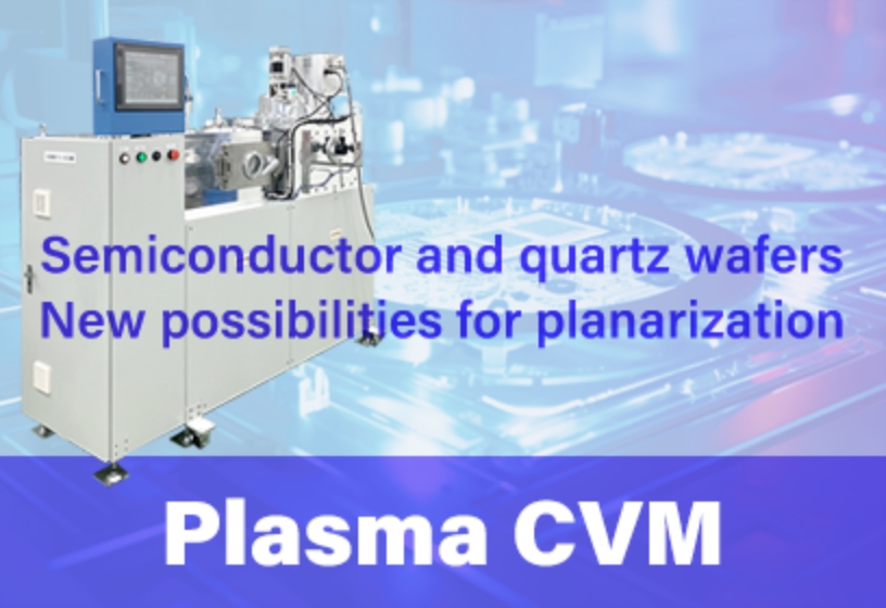

Plasma CVM
Vapor-phase chemical etching using high-density plasma realizes highly efficient yet distortion -free processing.
Processing object
SiO2 (crystal), Si, SiC
Application examples
・Uniform thickness of quartz substrate (TTV<10 nm)
・Uniformity of Si layer in the SOI thin film
CARE
A pad with catalytic functionality flattens materials on an atomic scale in a purely chemical manner.
Processing object
SiO2, Si, lithium niobate (LN), lithium tantalate (LT), etc.
Application examples
・Surface finish of LN substrate for SAW devices (Sa<0.1 nm)
・Surface finish of wafer and bonding (Si, SiO2, etc.) surfaces
・Improvement of junction reliability through cleanliness
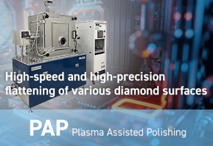
PAP
PAP accomplished in polishing a 20㎟ world- size class mosaic single-crystal diamond high-efficiently and damage-free.
Processing object
Diamond, Oxide Ceramics
Application examples
・High-speed polishing of diamond (polycrystalline and monocrystalline) (equivalent or better than SKAIFU)
・Creation of damage-free surface without altering the crystal structure, etc.
ECMP
Highly efficient polishing method utilizing an anodic oxidation reaction with ion-conductive polymer pads.
Processing object
SiC
Application examples
・High-speed polishing of SiC wafers (6µm/Hr or more)
・SiC wafer surface finishing (Sa 0.5nm or less)
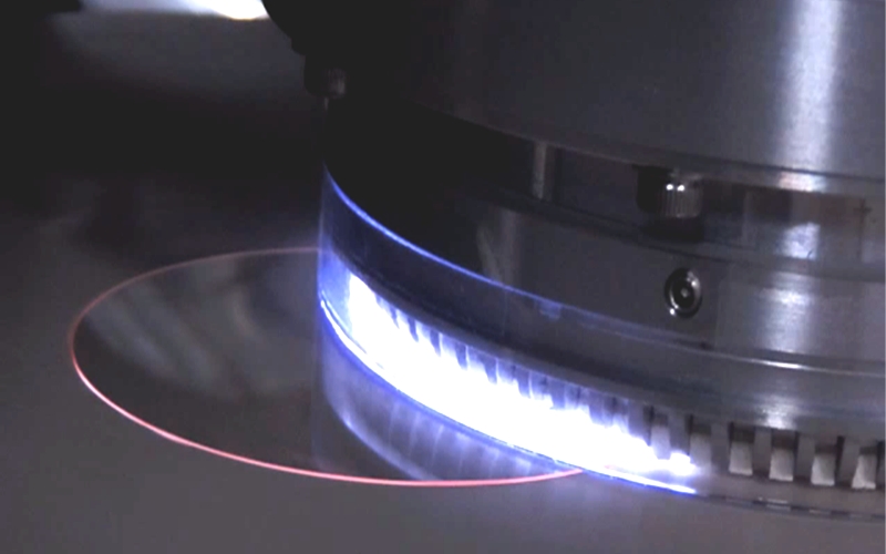
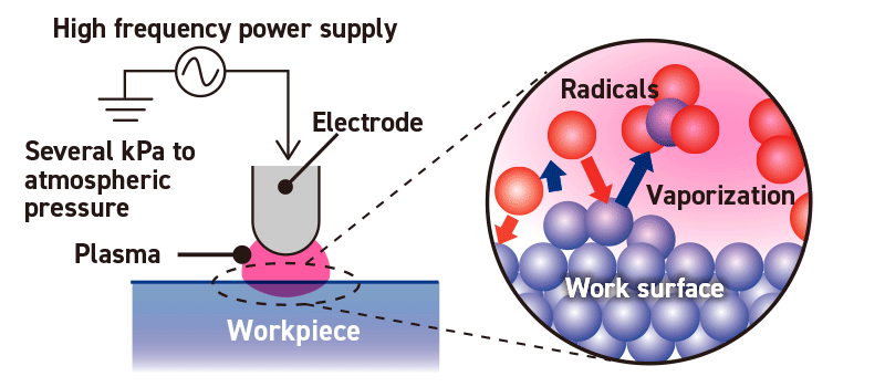
Plasma Chemical Vaporization Machining Method
Plasma CVM
Plasma CVM (Chemical Vaporization Machining) is a dry etching technique that uses plasma under several kpa to an atmospheric pressure. High-density, highly reactive radicals are generated locally to chemically etch atoms on the surface of the workpiece. Because the amount of processing can be controlled locally according to wafer thickness variation, it is possible to suppress thickness variation of 10 nm or less (TTV), which has been impossible with conventional processing methods. This method is used for processing Si wafers and quartz wafers.
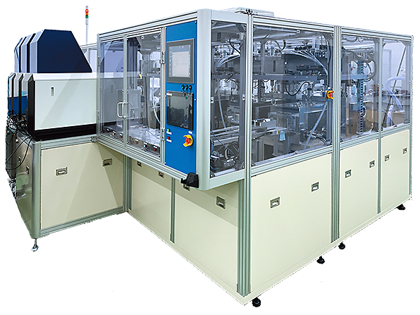
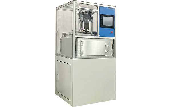
JC2000 System
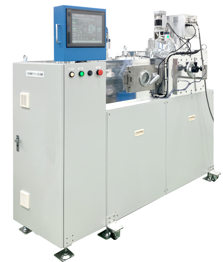
JC100 (Stand alone)
Processing Principle
Plasma Chemical Vaporization Machining technology
■Features
Realization of “uniform wafer thickness and planarization” and “thinning of thin film layers and bonding layers,” which were impossible to achieve with conventional processing methods.
■Typical application examples
・Uniform thickness of quartz substrate (TTV<10 nm) ・ Thinning the Si layer of SOI
■Sales Results
・Crystal wafers
Quartz wafer
Pre-processed Quartz wafer
4-inch (100 mm)/Commercially available
Measurement area:
Area within a circle 100 mm in diameter
TTV: improved from 102 nm to 18 nm
Thickness distribution
Before NC-Plasma CVM
Thickness distribution
After NC-Plasma CVM
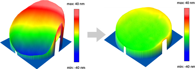
TTV: 102 nm
TTV: 18 nm
SOI wafer
Pre-processed SOI wafer:
8-inch (200 mm)/Commercially available
Thin film SOI wafer (SOI layer: 100 nm, embedded oxide film layer: 200 nm)
Measurement point:
Area within a 190 mm diameter circle, 5.5 mm grid
Average film thickness: further reduced from 97.5 nm to 7.5 nm
TTV: improved from 9.4 nm to 3 nm
Realization of ultra-thin layers that cannot be achieved by CMP
SOI layer thickness Before NC-Plasma CVM
SOI layer thickness After NC-Plasma CVM
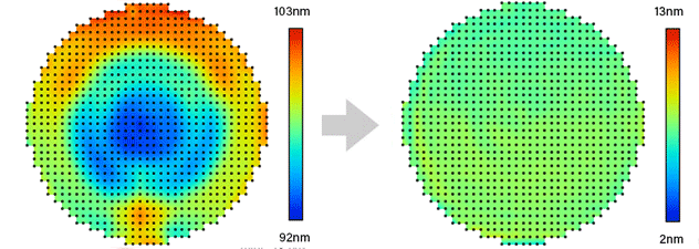
Average coating thickness: 97.5 nm
TTV: 9.4 nm
Average coating thickness: 7.5 nm
TTV: 3 nm
Ultra-thin wafer and highly uniform thickness is realized
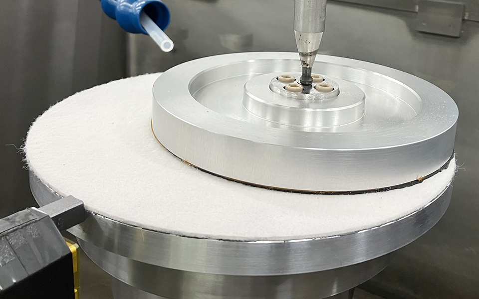
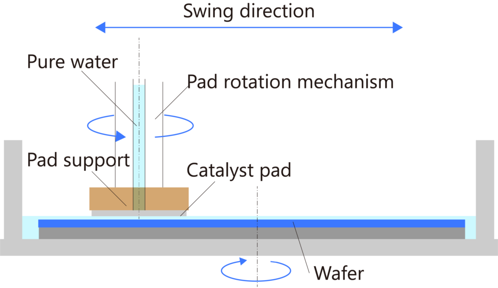
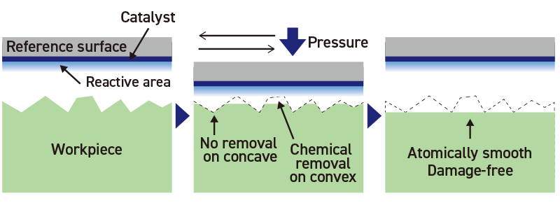
CAtalyst Referred Etching Method
CARE
CARE (CAtalyst Referred Etching) is an atomically advanced process using only pure water with metal catalyst action to achieve a surface roughness (RMS) of 0.1 nm or less.
It is used as a final finishing process after surface processing such as CMP* and is applied to improve the performance of LT/LN wafers for SAW devices by mirror finishing and to improve the reliability of bonding by mirror finishing the base substrate of bonded devices.
*CMP: CMP polishing method (Chemical Mechanical Polishing)A polishing method that mechanically polishes the surface of a wafer using a pad and chemicals containing abrasive.
CA1000
CARE Main Unit
Equipment Schematic
Processing Flow
■Features
Creation of “ultimate atomic-order surface” and “surface with no altered or modified layers” as the final finish after polishing processes such as CMP
■Typical application examples
Surface finishing of LN substrates for SAW devices (Sa<0.1 nm)
Surface finishing of wafers before bonding for bonding devices
Examples of CARE-processed surfaces
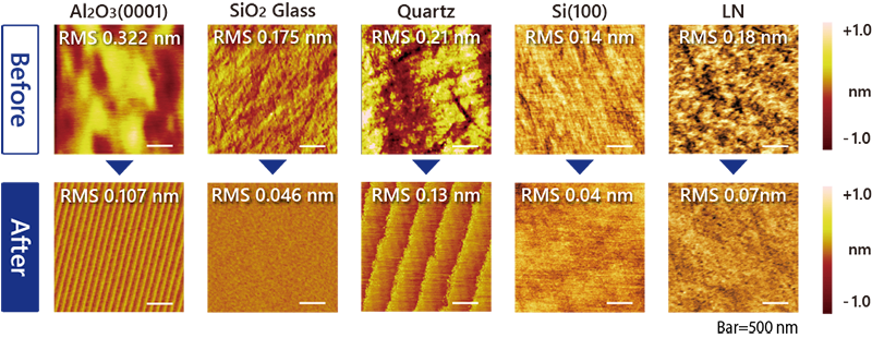
Atomically smooth and damage-free surfaces
High potential and applicability to semiconductor material polishing
Plasma Assisted Polishing Method
PAP
PAP (Plasma Assisted Polishing) process is a unique polishing process that uses plasma to modify the surface of the workpiece/seal and is specialized for polishing hard materials such as diamonds. It is more efficient than mechanical polishing using conventional diamond abrasives, etc., and produces a surface with less damage and defects. It is expected to be used in the processing of diamond substrates, which are attracting attention as power devices in the future.
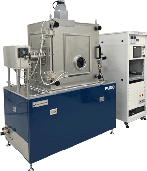
PA1100
Equipment Schematic
Polishing technology with the aid of chemical action by plasma
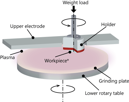
*e.g.,Diamond substrates
Before and after PAP on single crystal diamond
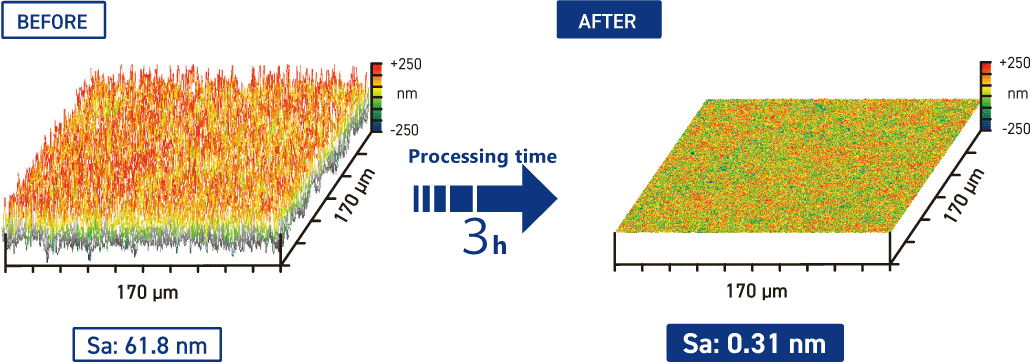
Sa: improved from 61.8 nm to 0.31 nm
By Atomic Force Microscope
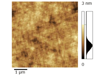
Surface roughness: 0.36 nm rms
By Confocal Raman Microscope
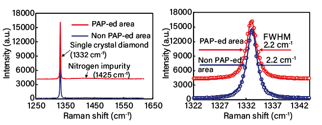
No disturbance of crystallinity or change to graphite structure
■Features
“Highly efficient and damageless polishing of hard materials” replacing conventional processing methods (e.g. scaife polishing)
■Typical application examples
High-speed polishing(equivalent or superior to Scaife) of diamond (polycrystalline and monocrystalline)
Damageless polishing without any change in the crystal structure of diamond
■Sales results
Diamond materials and substrates
Plasma CVM, CARE, and PAP are proprietary technologies of The University of Osaka.
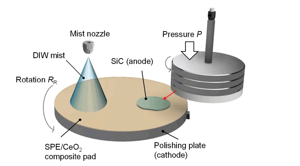
Electro-Chemical Mechanical Polishing
ECMP
Ideal for highly efficient polishing of SiC as an alternative to CMP
ECMP (Electro-chemical Mechanical Polishing) processing is a method focused on SiC polishing and was developed as an alternative process to lapping/CMP. It uses anodic oxidation for polishing , but does not require an electrolytic solution. By employing ion-conductive polymer pads, it is a safe and environmentally friendly process that avoids the use of chemicals. 6 μm/Hr processing rate has been obtained.
Equipment Schematic
Processing Flow
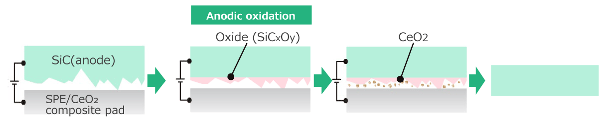
Utilizes the phenomenon of anodic oxidation (softening) of the workpiece surface
No chemical solution is required due to the use of ion-conductive pads
■Features
・”High-speed, precision polishing” and “low environmental impact processing without using chemicals” as alternative polishing technology to CMP
■Typical application examples
・High-speed polishing of SiC wafers and surface finishing of SiC wafers
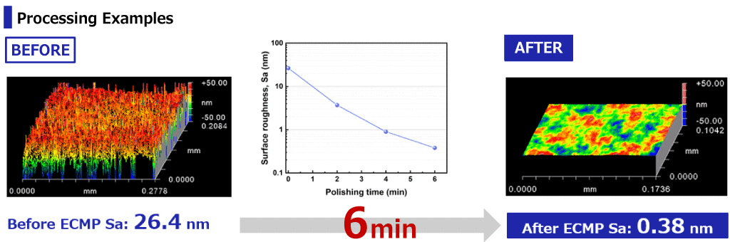
Processing rate
This method 6µm/Hr
Processing example: Sa change after 6 min
Ideal for highly efficient polishing of SiC as an alternative to CMP
ECMP is a proprietary technology of Ritsumeikan University
JTEC Corporation’s Strengths in developing automated system
Providing our proprietary nanoscale surface processing and modification processes
・Our proprietary processes that can be controlled at the nanoscale and atomic level.
・We propose the best processing method according to the workpiece material, requirements, and purpose
(we have four proprietary processes: Plasma CVM, PAP, CARE, and ECMP).
Consistent support system from R&D and small-lot prototyping to mass production
・Support for each customer’s stage from basic research to small-lot production and mass production
・Customized support from experimental machines and small-lot production machines to automatic machines for mass production is available.
Close collaboration with universities and research institutions
・Promote ongoing joint research with the Graduate School of Engineering, The University of Osaka
・Expansion of university-originated cutting-edge technology into the industrial world
Terms related to semiconductor materials
| Quartz Wafer | It is a wafer made of transparent crystals, primarily composed of quartz (SiO2), and has the property of transmitting high-frequency signals in a regular and stable manner. It is mainly used in fields such as electrical equipment, optical communications, sensors, and clocks. |
| Diamond Substrates | It is a substrate for electronic components based on artificially synthesized diamond, which has high thermal conductivity and electrical insulation properties. It is expected to be used in a wide range of fields, such as trains and automobiles, which require further acceleration of calculation processing and communication speed of information terminals and control of high-current power. |
| SOI Wafer | Abbreviation for Silicon On Insulator (SOI) wafer, a wafer with two layers: a silicon layer and a silicon oxide layer (insulating layer). SOI wafers are innovative semiconductor wafers developed to meet requirements for low power consumption, high integration, and high-speed operation. They have recently been used in mobile devices, IoT devices, automobiles, medical devices, and other fields. |
| Power Semiconductors | These elements are indispensable for the construction of highly efficient power conversion systems. For example, inverters using power semiconductors are used to convert DC power obtained from solar and wind power generation into AC power. Control systems using power semiconductors are also used in automobiles, railroads, and other forms of transportation. |
| SAW Filter | They are electronic components that can remove unnecessary signals in electronic circuits and are widely used in, for example, smartphones, GPS receivers, and digital TV receivers. In particular, miniaturization and power saving are progressing, and demand for mobile terminals and IoT devices is increasing greatly. |