New project
Applying our advanced surface nano-manufacturing technology, we are developing new business of the semiconductor, space, and medical fields.
Joint development with partner companies
For launching a third new business following optical and life science business, we are developing new application based on our nano-technology (EEM nano-processing and RASDI / MSI nano-measurement)to other industrial fields.
- Optical elements for next-generation semiconductor manufacturing and evaluation equipment
- Optical element for X-ray microscope
- Nano-processing & measurement for high-precision mask substrates
For commercializing new nano-processing equipment “PCVM”, we are working on joint development with partner companies in the following fields.
- Quartz crystal wafer processing and inspection device
Furthermore, based on the cell culture technology with long experience in regenerative medicine, we are developing not only sales of automation cell culture system but also providing cell culture support service related to regenerative medicine.
- Support services for regenerative medicine.
Our surface nano-processing technology
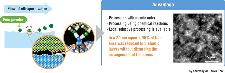
Elastic Emission Machining (EEM)
EEM is a unique surface nano fabrication technology that uses chemical reactions between the fine particles and the surface of the workpiece.
In this method, we use special fine particles that react with the surface atoms of the object in ultra pure water. By acting on the surface of the workpiece to remove the upper layer, an ultra flat perfect surface at atomic level is realized.
- Process principle of EEM
-
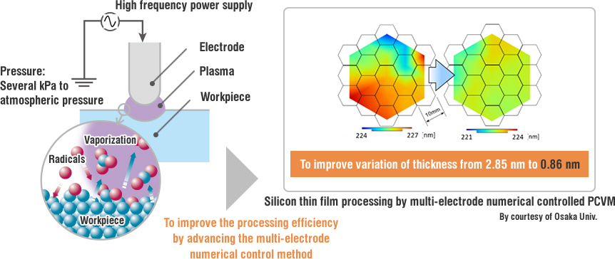
Plasma Chemical Vaporization Machining (PCVM)
PCVM is a dry etching technology using plasma at atmospheric pressure. In this process, high-frequency plasma is generated around the electrode for generation of high-density and highly reactive radicals locally. Reaction of the workpiece surface atoms with plasma generates volatile substances.
PCVM is not affected by equipment accuracy because numerical processing controls the processing volume using the plasma residence time. There is no disturbance of the atomic arrangement on the workpiece surface.
In addition, we aim to further improve the processing efficiency using a multi-electrode numerical control method: a unique technology created at Osaka University, to provide practical applications.
- Process principle of PCVM
-
High-efficiency strain-free machining is realized by chemical etching using high-density plasma
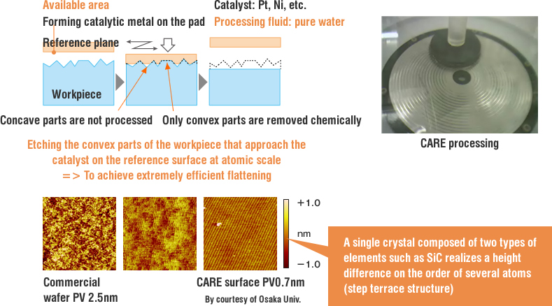
Catalyst Referred Etching (CARE) Technology
CARE is a unique etching technology that uses catalytic action to chemically remove only the convex portions from the surface to be processed. A pad with a catalytic function formed of Pt or Ni is moved on the workpiece with ultra-pure water as the machining fluid. It flattens the surface of various materials, such as glass and SiC, at atomic scale.
With our EEM nanotechnology, it is possible to realize extreme flatness of four layers of Si atoms (P-V 1nm) on workpieces used for a 1m-long mirror. CARE technology aims to realize the flatness for a single layer of Si atoms (P-V 0.7nm) , which is the ultimate processing method.
- Catalyst Referred Etching (CARE) technology
-
Using a pad with catalytic function to flatten the surfaces of various materials on an atomic scale.